Hacker Summer Camp 2017: XXV Badge
In my post the Many Badges of DEF CON 25 I may have not-so-subtly hinted that there was something I was working on. While none of the ones I listed were created in response to the announcement that DEF CON had been forced to switch to “Plan B” with their badges, mine more or less was. Ever since I saw the Queercon badge in 2015, I’d had the idea to create my own electronic badge, but the announcement spurred me on to action.
However, what could I do in only 2 months? Before I created this badge, I had never created a PCB. All my electronics design work before had been on protoboards at best, and while I had assembled SMD electronics on PCBs before, I had no idea how to design with it. So, it seemed like a perfect learning opportunity.
Boy, did I ever learn. In the process of creating this badge, I created 3 separate sets of PCBs, soldered 7 finished badges, (yes, only 7 – maybe this was the most exclusive unofficial badge?), debugged numerous problems, and read way more datasheets than I expected I would.
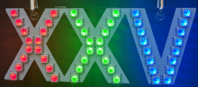
So what did I come up with? Well, how does 48 RGB LEDs drawing up to 15W of power sound? Overkill? It totally was.

Ok, maybe there’s a little too much glare there. Sorry. It turns out that pointing a cell phone at 48 LEDs rarely results in a quality photo. Let’s try it again without the blinding light.

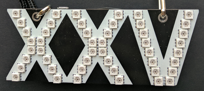
Way better, don’t you think? This is the “XXV Badge” – 48 APA102C LEDs controlled by a Atmel SAMD21 ARM Cortex M0 MCU clocked at 48 MHz. The SAMD21 runs at 3.3v, the LEDs at 5V, so I have a boost converter driving the LEDs based on a TPS61232. A 74AHCT125 quad buffer provides level conversion (though not really designed to, it works quite well) for the SPI signals. All told, there’s 98 components, though many of them are simply things like decoupling capacitors.
I know the design is simple, but I’m no artist. On the other hand, I feel like it worked out quite well for the parties and I got a number of compliments and interest in the badge, so I’m pretty happy with the outcome for my first badge design (and first PCB!) I can’t wait to start thinking about next year!
The boost converter design & layout are approximately based on the reference design from TI, but I had to make a few adaptations due to part size and layout constraints. Fortunately, it ended up working out pretty well, and with fresh batteries, the output is well-regulated. However, running all of the LEDs at full brightness draws more current than 3xAAAs can support, causing the input voltage to the boost converter to drop and resulting either in an immense amount of ripple, or so much dropout that the SAMD21 CPU resets.
Kicad design files and firmware source code are on GitHub! My production boards were produced by Hackvana.