Course Review: Applied Hardware Attacks: Rapid Prototying & Hardware Implants
Over the past 4 days, I had the opportunity to take two hardware security classes taught by Joe Fitzpatrick(@securelyfitz) along with @_MG_. Both courses are part of the “Applied Hardware Attacks” series of courses taught by Joe. The first course, “Rapid Prototyping”, is focused on using 3D printers and PCB mills to build interfaces to hardware systems. The second course, aptly named “Hardware Implants” applies these skills to build hardware implants to perform attacks on hardware systems. Both courses are very timely and informative, as well as a lot of fun.
I really like Joe’s teaching style – he provides just enough guidance through lecture for you to have an understanding of the problem space and the possible solutions, then turns you loose on problems to be solved. His lab manuals generally provide enough information to be clear without giving you mere steps to be reproduced. Rather, you need to think about the objective and perform analysis and problem solving yourself.
It’s worth noting that this was Joe’s first time offering both of these classes, and while there were some rough edges, I really enjoyed the courses and thought they were a great use of my time and a good way to expand my skillset and get a better understanding of what is possible in terms of hardware attacks. Because this was his first run through, it’s likely that later deliveries might be significantly different from my experiences.
While Joe offers these two courses independently and did not strictly enforce any prerequisites, you really should take the two classes together. If you do not know how to operate 3D printers and PCB mills, you will be severely disadvantaged in the Hardware Implants course. Likewise, since both classes involve some CAD software, if you have a preferred mouse, do bring it. EDA software is not fun with a touchpad, as I discovered the hard way.
Rapid Prototyping
Rapid prototyping introduces the idea of making hardware interfaces to connect to interfaces on your target device. Most often, this seems to be pads on the PCB, such as a UART, JTAG, or other debug interface. Sometimes these will be test points that are not arranged in a particular standard interface, or you do not want to solder to the target board, so need a mechanism based on contact alone.
Joe dealt well with a major curve ball while teaching this class. We began the first day with only 2 students in the course, and I was looking forward to the 1:1 student:instructor ratio. However, around lunch time, another instructor became ill and could not continue. His students were offered a refund or to switch to another course, and 5 students ended up switching into this class. It was obviously a little bit of a strain for the class to go from 2 to 7 so suddenly, but Joe handled it well and I think it worked out just fine.
At a high level, two main tools was introduced for building attack interfaces to our targets. The first, 3D printing, is probably familiar to everyone, but PCB milling may not be. PCB milling is the use of a computer-controlled mill to mill away the area between traces and other desired areas on a circuit board. Both tools allow us to produce something that will hold spring-loaded electrical contacts (“pogo pins”) in contact with our target device.
 {:.left}
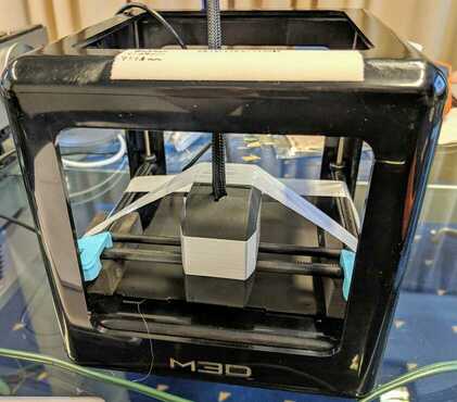
For the printer, we used the Micro by M3D, which is a relatively small 3D printer. Joe specifically stated that he does not recommend this printer unless your use case is the same as his: specifically, a 3D printer that can be placed in checked luggage and be up and running quickly at his destination. The injection molded plastic (probably polycarbonate) housing was very rigid, which is good for both print quality and sturdiness in shipping. However, the actual extruder and movement mechanisms seem relatively low quality and have significant play in them. The print bed is plastic (and not a particularly rigid one) and the printers Joe brought all had a small amount of upward bend to them. Joe recommended alternatives based on reviews he’d read, but not personal experience.
 {:.right}
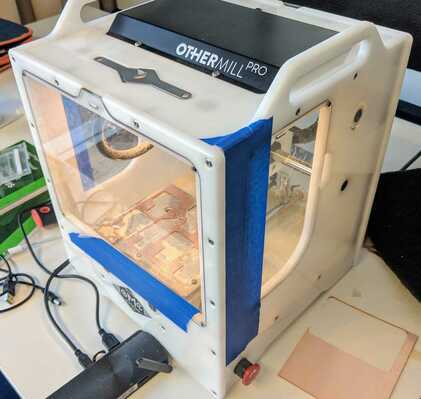
The PCB milling machine in use was an Othermill Pro, a tool whose design is now owned and produced by Bantam Tools. This tool was incredibly impressive and could produce some really sharp looking PCBs. We tried to stick to using a single bit size to avoid bit changes, but some tasks required a more precision approach. However, even for pins on 2mm centers, we had no trouble milling with a 1/32" end mill. (Yes, the mill pretty much only uses imperial units as far as I could tell during the 4 days.) If it weren’t for the noise and dust (and possibly the price tag) I’d be all over one of these. The idea of being able to have PCBs in hand in a few minutes is very attractive.
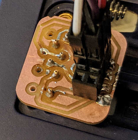
In the course, we predominantly focused on two targets: one was a small development board with JTAG pins near the end, and one was an AVR-based consumer device with ICSP pins available through the plastic enclosure. Most of us chose to go with 3D printing for a jig for the development board and milling a PCB to hold pogo pins in the right place for the consumer product.
Since this was the first run through, there were a few rough spots. For example, the ICSP pinout listed in his lab manual had MOSI and MISO swapped. For some reason, programming doesn’t work so well if you have these pins swapped. :) I’ve been assured this will be fixed for future iterations of the course, but it’s a good reminder that double-checking pinouts against multiple sources is not a bad idea.
Because it is “rapid prototyping”, we were encouraged to try and iterate on our designs to get things to work correctly. This lead to the alternative names “reckless prototyping” and “rapid failure.” To be fair, these names aren’t wrong – I definitely started making things without being nearly as careful as I would be if I were sending a PCB out to a fab, and I definitely had lots of failures. In fact, it took 11 iterations to get a good 3D print for a jig for the development board. Part of it was trying to print sub-millimeter holes in the jig for pogo pins that are nominally 0.5mm in diameter. Part of it was my inexperience with 3D modelling. However, I eventually got both a milled PCB and a working 3D printed jig out of the class.
 {:.left}
 {:.right}
Hardware Implants
{:.clear}
The second class applies the techniques from the first class to build more complex devices – the ultimate goal being fully self-contained hardware implants that can carry out an attack on their own. (As opposed to being an interface to an attacker computer or similar as in the rapid prototyping course.)
This course was extremely open-ended. Joe provided a small survey of hardware-based implants, then showed off some implants he had prototyped for systems like PLCs as well as some implants from the NSA Playset project. He discussed the motivations for developing a full implant, how attackers might use them, and some of the options for automated functions. He then presented some problems for us to solve in the labs.
In this course we mostly focused on a single target (a Pogoplug device) but there were options for other targets as well. The target has an unpopulated UART header that has an unauthenticated root shell available on it. The goal was to develop an implant that leveraged this and did not require much time or effort to implant (e.g., no soldering, etc.).
Joe encouraged us to take an incremental approach to developing this implant:
- Build an interface (as in the first class) to connect to the UART pins. This will help verify the position/spacing of the pins as well as help determine the pinout. (GND, VCC, RX, TX)
- Build an implant with a microcontroller on it to conduct a fully automated
attack. (e.g., send a payload just after booting) This was to give a remote
shell over the network on the device (using, e.g.,
nc). - Prototype an implant that gives a wireless shell using the
ESP8266. This would provide an out of band shell (i.e., inspection of the software and process table on the device would not reveal any abnormality). - Build an implant that provides the wireless out of band shell and can be installed entirely within the original case of the Pogoplug. This would be an attack that would require disassembly to discover, as it would use its own wireless network and not have physical signs outside the case.
I actually skipped the 2nd step and went straight for the wireless implants after verifying my pinout. The first prototype was quite simple, as we were using a full ESP8266 dev board. It essentially required connecting 4 leads from the dev board to the interface board, and flashing a serial to wifi sketch on the ESP8266. I was happy that this worked on my first or second try.
On the other hand, I had nothing but problems with building the real implant. This was my first time making a board for a raw ESP8266 module (and it turned out it was also Joe’s first time working with the bare modules). At first, I used pins that affected the boot process, then we discovered that there are certain pins on the ESP8266-12F module that must be pulled up/down in order for it to boot properly. This resulted in several iterations of the board, with the final iteration housing 4 resistors (and some creative routing) to work.
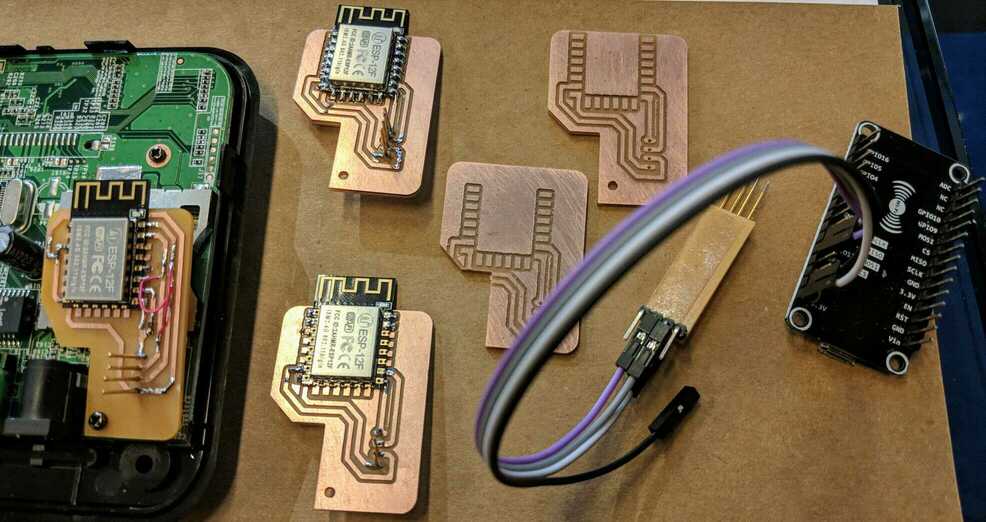
Another artifact of this being a first time class was a lack of some tools that would be useful. For example, I really like to have tweezers when soldering, but they were nowhere to be found. Likewise, the need to line up pogo pins neatly on boards would have benefited from a helping hands or a PCB vise. In hindsight, I should have just 3D printed something to support the PCB during soldering of the pins.
We wrapped up the class with MG showing off the iterations that have gone into the O.MG Cable. He provided a board from an early version (no wifi, simply an ATTiny85) to each student to solder into a USB A connector for a cable. I opted to skip this to keep working on the wireless implant, but it was obvious from other students that it required a lot of fiddly soldering.
Conclusion
Everyone learns in different ways. While Joe is happy to provide as much help as a student needs, his general approach probably caters most to those who learn by doing. Lecture is light and most of the learning happens during the lab segments. He gives enough space that you will make mistakes and fail, but not so badly that you never accomplish your objective. If you read the lab manual carefully, you will find adequate hints to get you in the right direction.
On the other hand, if you’re a student that wants to site in a classroom and listen to an instructor lecture for the entire time, you are definitely in the wrong place. If you do not work on the labs, you will get very, very, little out of the course.
The rapid prototyping course is a good introduction to using the 3D printer and pcb mill for hardware purposes, and would be valuable even for those building hardware instead of breaking it. It really opened my eyes to the possibilities of these technologies. On the other hand, I suspect that the hardware implants course has limited application. It’s useful to learn what is possible, but unless you work in secure hardware design or offensive security that would use hardware implants, it’s probably not something directly applicable to your day to day.
The classes were both very fun, so if you want something to learn “just for fun”, these would be a great way to go. You should be conceptually familiar with UART and JTAG interfaces, and having designed even a simple PCB before the class will really help you with the tools. Unfortunately, Joe uses Eagle for PCB design, but he claims he’ll be adding KiCad directions to the course as well (there were placeholders for this in the manuals).
Overall, I think the courses were a great opportunity to learn something very enjoyable. While it’s possible that you could figure out most of the material on your own, it’s so much more efficient (and fun) to have someone provide pre-calibrated tools, labs thats are designed to help you get going, and support when you hit a road block. I would recommend these to anyone interested in seeing how hardware implants might work and who has at least a basic understanding of electronics, printed circuit boards, etc.